Tips and Tricks for Using PCB Footprints and Symbols
Historically, engineers would spend days making PCB symbols and footprints from scratch, a tedious and time-consuming process. To make life easier during board layout—and to help engineers get their products to market faster—CUI Devices teamed up with SnapMagic (formerly known as SnapEDA) to deliver high-quality models that have gone through multiple stages of verification.
The PCB symbols and footprints encompass our range of audio, interconnect, sensors, switches, and thermal management products and are free to download from our website or from SnapMagic Search. This blog aims to take a look at some of the key features of these PCB symbols and footprints, their standards and verification process, as well as other tips and tricks to speed up the design process when designing with CUI Devices’ products and SnapMagic.
What is SnapMagic?
SnapMagic is the first and leading electronics design search engine. Their mission is to break down barriers so engineers can innovate. Each year, a million engineers build their products with SnapMagic's PCB symbols and footprints to save time and innovate faster. Their latest Copilot tool, powered by AI, allows engineers to design even faster by auto-completing circuit board designs with helpful recommendations.
How to find PCB models on CUI Devices’ website?
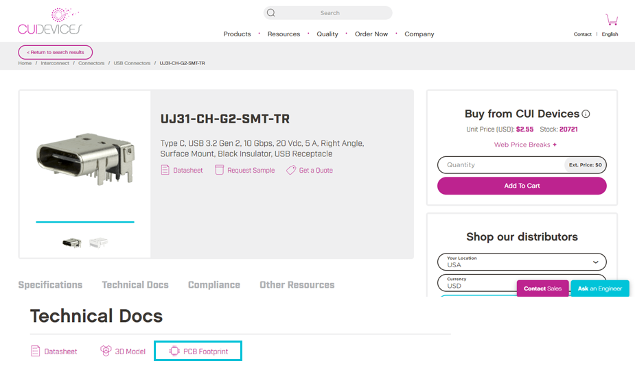
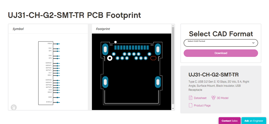
There are several ways to access PCB footprints and symbols on www.cuidevices.com. If the specific model number is known, simply type it in the model number/keyword search to navigate to the product page. Shown in the image below, a link to the PCB footprint viewer can be found in the "Technical Docs" section of product pages.
PCB symbols and footprints can also be accessed through CUI Devices’ CAD model library. This helpful resource houses all our 3D models and PCB footprints in one convenient location. Simply search by model number or filter by product category and type to access the available models for a given product.
What PCB design formats are supported?
CUI Devices’ PCB symbols and footprints can be downloaded in all major PCB design formats, including Altium, Eagle, KiCad, OrCAD and Allegro, PADS, and PCB123. Simply select the format at the top right-hand corner to start downloading for the desired PCB design tool.
How do I import the files I downloaded?
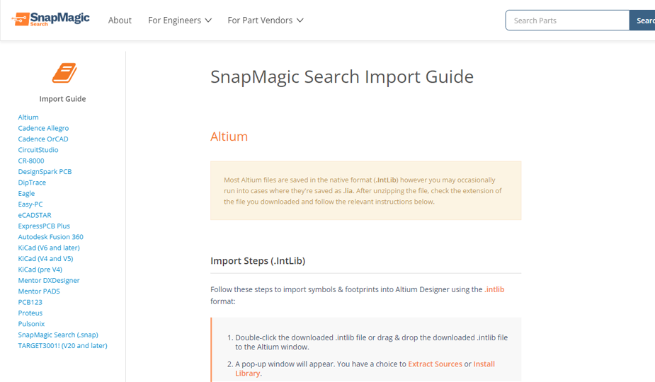
Upon download, there will be a .zip file containing a file called how-to-import.htm. Double-click on that file to be referred to the SnapMagic Search Import Guide. From there, select the desired design tool on the left-hand navigation panel. This Import Guide contains all the required tutorials and instructions needed to import.
What standards do the models follow?
The PCB footprints follow CUI Devices’ recommended PCB layouts from our datasheets, as well as key aspects of the IPC-7351B and IEEE-315 standards, where applicable.
How are the models verified?
All models follow a three-step verification process undertaken by SnapMagic. This includes having multiple engineers reviewing the content, as well as verification through their proprietary patented symbol and footprint verification technology.
Additionally, all models are verified by our engineers at CUI Devices as a final step in the process between the two companies.
With that being said, it is always necessary that engineers verify that the models meet their unique design environments and requirements before manufacturing.
Can these models be used for commercial designs?
Yes, these models can be used for the purpose of designing circuit boards by professional designers. The models are licensed under the Creative Commons Attribution-ShareAlike 4.0 International License (CC BY-SA) with the Design Exception 1.0.
SnapMagic introduced the concept of the Design Exception back in 2015. It allows the CAD models to be used for commercial purposes with full freedom and flexibility. As per the Design Exception:
You have permission to propagate a work of a design, design file(s), and/or manufactured board(s) formed by combining CAD symbols and footprints provided by SnapMagic, even if such propagation would otherwise violate the terms of CC BY-SA. You may then convey such a combination under terms of your choice.
For full details, please refer to the license included with the models.
Other Frequently Asked Questions
*Tool not yet officially supported by SnapMagic, please verify upon import.
More PCB Design Tips and Tricks
- Build a project library on SnapMagic using CUI Devices products, as well as other complementary parts in a design. Users can then batch export that library of CAD models for their project as one single library.
- Use computer vision and artificial intelligence to automate symbols for other integrated circuits in a design using InstaBuild, completely free.
- Download the SnapEDA plugin for tools like Altium, KiCad, and Eagle which allows engineers to search and download CAD models right within the design tool.
- Request CAD models that do not yet exist in the SnapMagic Search library in 24 hours via the InstaPart service.
Conclusion
Circuit board design has historically been a time-consuming and challenging process due to a variety of product configurations and standards. However, by following the tips and tricks outlined in this blog and utilizing CUI Devices’ vendor-verified PCB footprints and symbols, users can prevent footprint errors and design smarter.
Additional Resources